GF180 D-type Flip Flop

Introduction
This circuit demonstrates a negating D-type Flip Flop implemented on the Global Foundries 180nm process node. This Flip-Flop acts as a memory cell, holding a single bit upon falling clock edge. The bit is read in from the D node and constantly output upon the Q node.
In digital logic, the circuit can be represented as: 
The circuit netlist is contained within the gf180_dff.spice file in this directory. To begin running the simulation harness, open the gf180_dff_transient.jl file and begin running statements.
Files
gf180_dff_transient.jl- simulation harnessgf180_dff.spice- circuit netlistgf180mcu_fd_sc_mcu7t5v0__dffnq_4.ngspice- detailed circuit netlist
Analyses
Transient
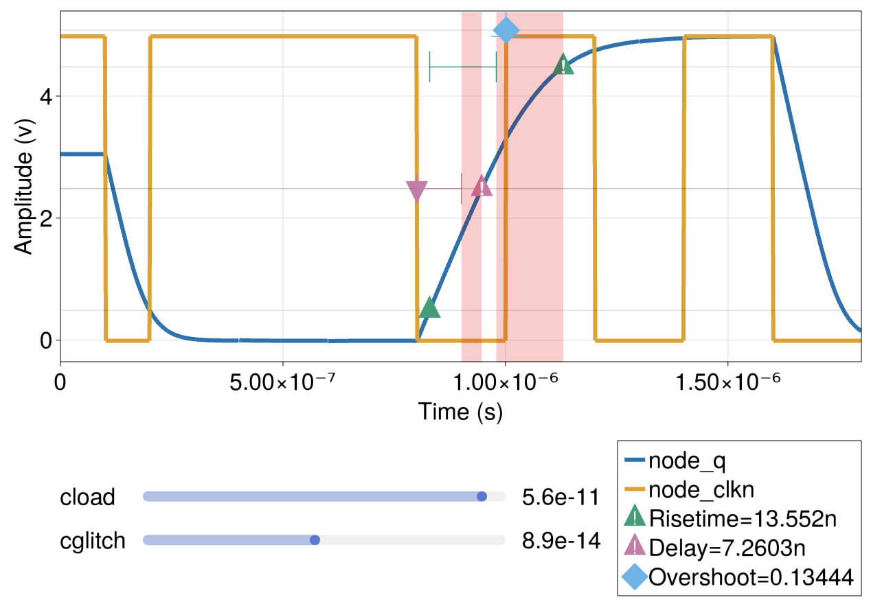
In this test we display only the clock and the output, as the input is not very interesting. Note that we have three checks being displayed, showcasing a parameter configuration that breaks some of the constraints.
When running the checks() function, a tabular display of all parameter configurations is shown, CTRL-clicking (or CMD-clicking on Mac) on any of the cells will display that particular configuration in the plot pane.
API Reference
- Configuring Parameters
- Simulating
- Exporting Results